For decades, scaling down process nodes has been the name of the game in the semiconductor industry. Physical limitations have challenged this trend, however, forcing semiconductor fabs to take new approaches to prolong Moore’s law.
TSMC has emerged as the world’s leading fab, besting Intel and other chipmakers with the most advanced 5nm node. Last week, TSMC made headlines when it announced a number of new innovations including the mass production of the N3 node, a new architectural innovation called FINFLEX, and a look ahead at its N2 node.

Pictured is a 3-2 FIN configuration, made possible by N3 with FINFLEX. Image (resized) used courtesy of TSMC
TSMC’s 3nm Node and a New FINFLEX Architecture
At the North American Technology Symposium, TSMC announced that its 3nm (N3) node would enter volume production in late 2022.
According to TSMC, the N3 node is the most advanced process node in the industry and will bring with it significant improvements for designers. Compared to TSMC’s 5nm node, N3 is expected to enable up to 70% gain in logic density, up to 30% power reduction at the same speed, and up to 15% improvement in speed at the same power. The result, TSMC said, will be cheaper, more performant, and lower power offerings for its customers.
A major component of N3 (and future nodes) is a new architectural innovation called FINFLEX.

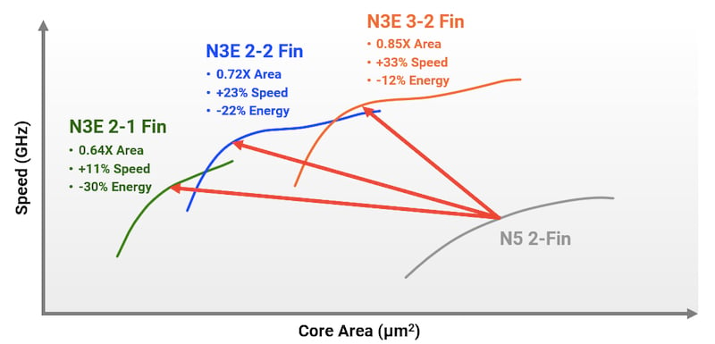
FINFLEX is said to optimize functional blocks as needed. Image (resized) used courtesy of TSMC
FINFLEX is described as a new methodology that combines process and design innovations to lend designers unprecedented flexibility on the N3 node. With FINFLEX, designers may choose their gate-all-around (GAA) transistor architecture on a block-by-block basis such that each functional block can be optimized for its given needs. FINFLEX allows designers to choose between a 3-2 FIN, 2-2 FIN, and 2-1 FIN configuration.
According to TSMC, the 3-2 FIN option is optimized for high-performance computing with fast clock frequencies, 2-2 FIN is optimized for a balance between power and performance, and 2-1 FIN is optimized for power efficiency, low leakage, and high density.
TSMC Scales Down to 2nm
Beyond N3 with FINFLEX, TSMC also introduced its future 2nm (N2) node.
TSMC’s N2 technology is said to take performance and efficiency to another level—beyond even the N3. N3 is reportedly going to be TSMC’s first process node to leverage gate-all-around field-effect transistors—GAAFETs—which TSMC refers to as nanosheet transistors. GAAFETs will be developed using EUV lithography tools from ASML. Along with the switch to GAAFETs, N2 is set to introduce technological improvements such as backside power delivery, a new methodology in power distribution that aims to minimize parasitics during power delivery to the transistors.
TSMC claims its N2 technology will offer speed improvements of 10–15% at the same power or 25–30% power reduction at the same speed compared to N3. N2 is still a long way from development with production scheduled to begin in 2025.

