INSPECTION BEFORE SHIPMENT
Check the corresponding incoming goods information, non-genuine products cannot provide traceable proof.
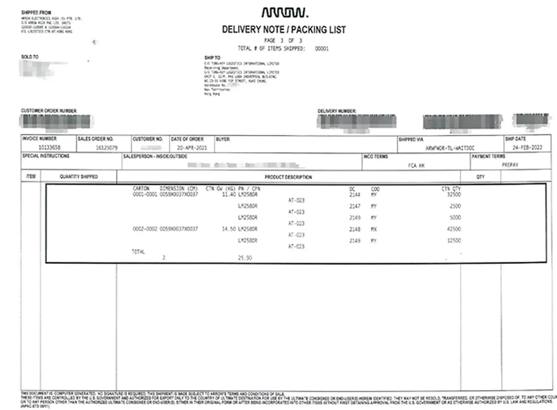
Example of agent shipment document

Check the corresponding incoming goods information, non-genuine products cannot provide traceable proof.
Example of agent shipment document
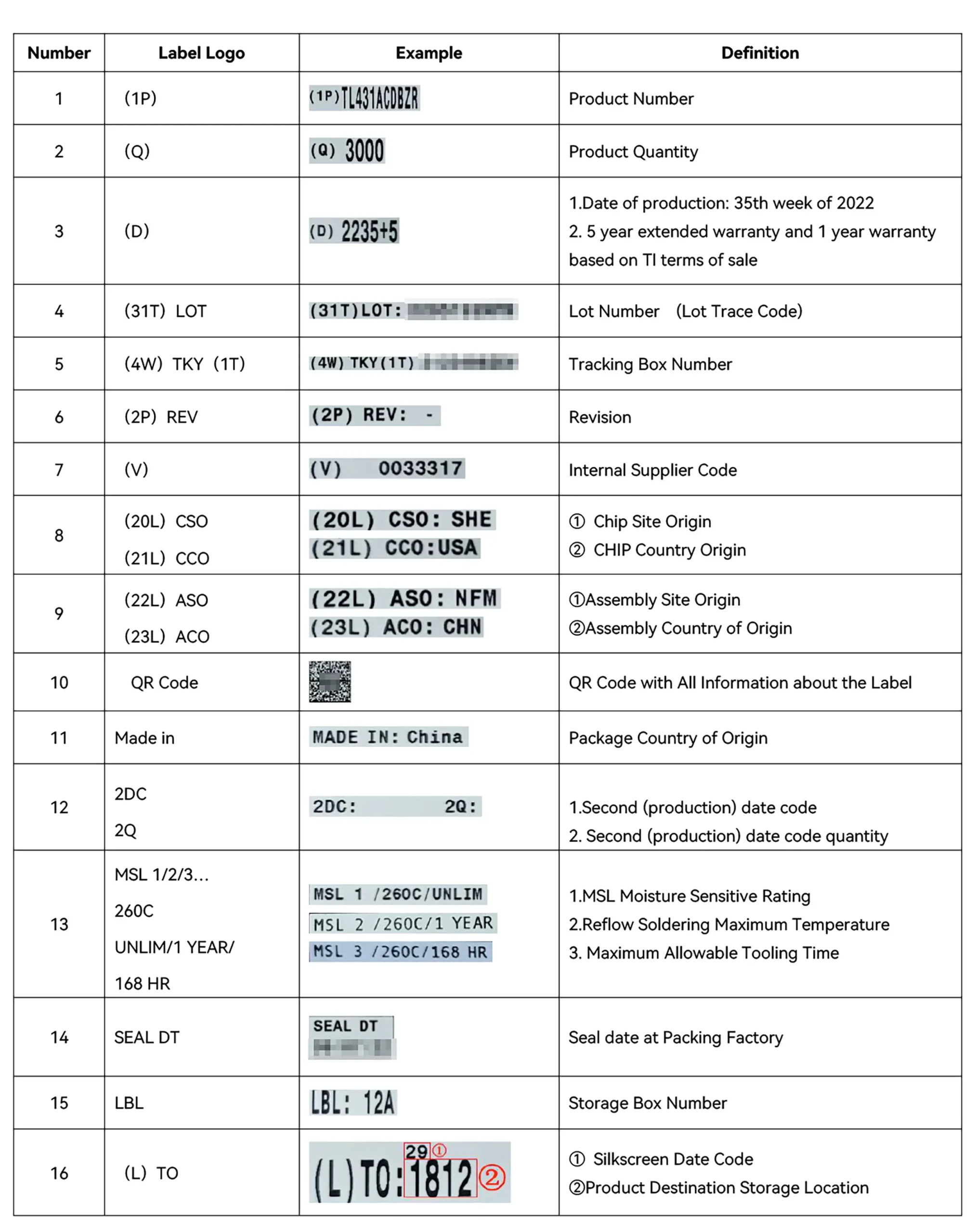
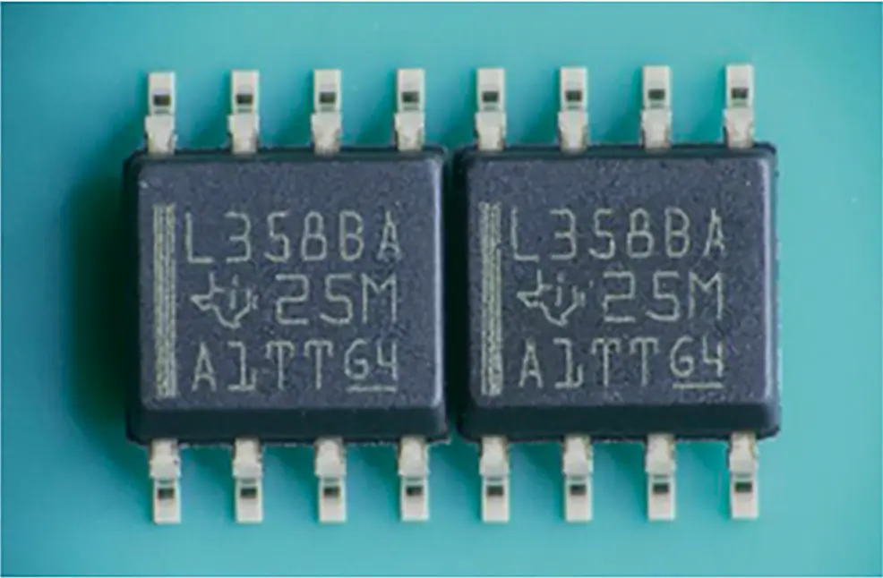
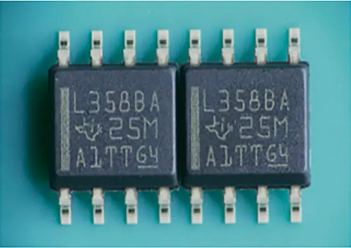
Label interpretation
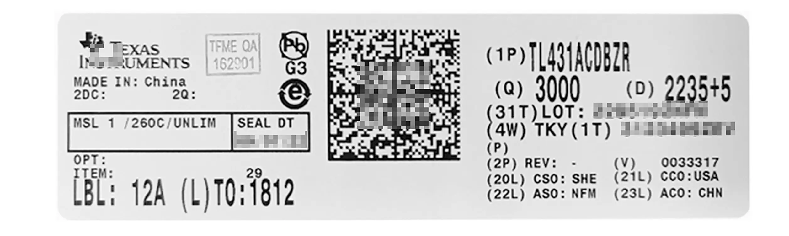
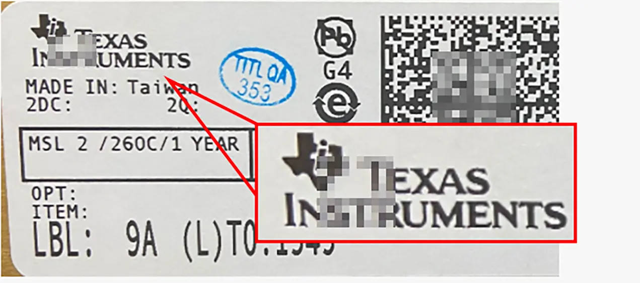
The LOGO printing font is an artistic font with curved ends.
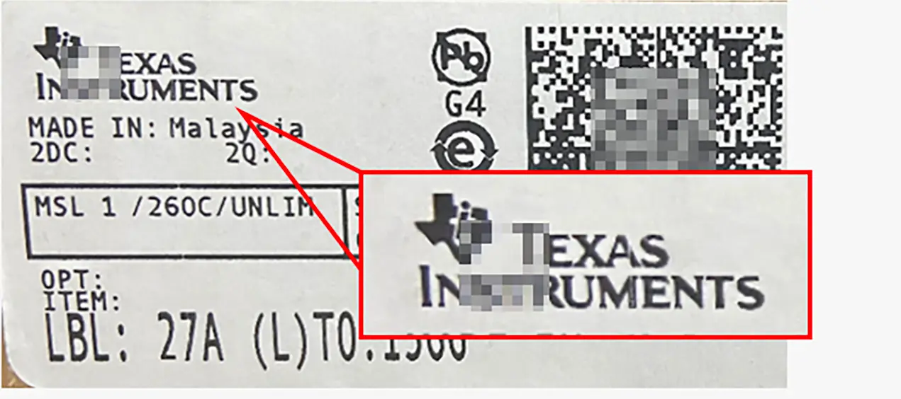
The details of the end of the font can not be restored one-to-one, with the help of magnifying glasses and other tools can be identified.
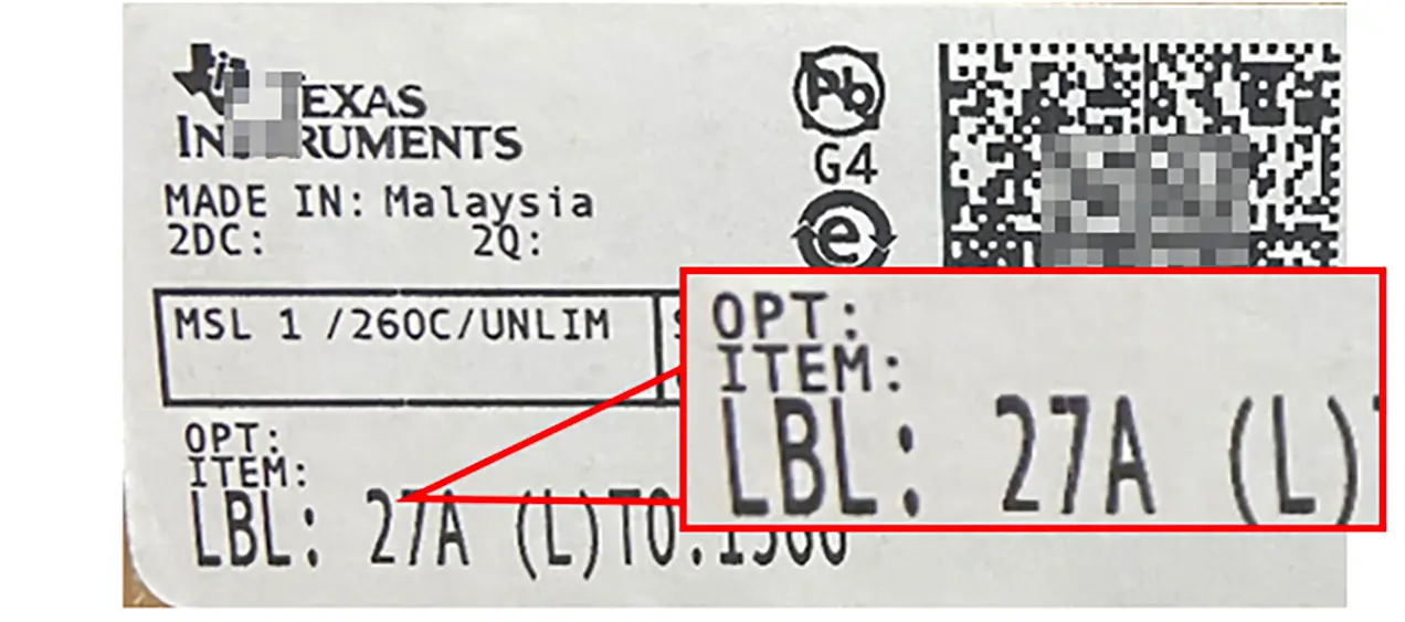
Printed line spacing in the lower left corner
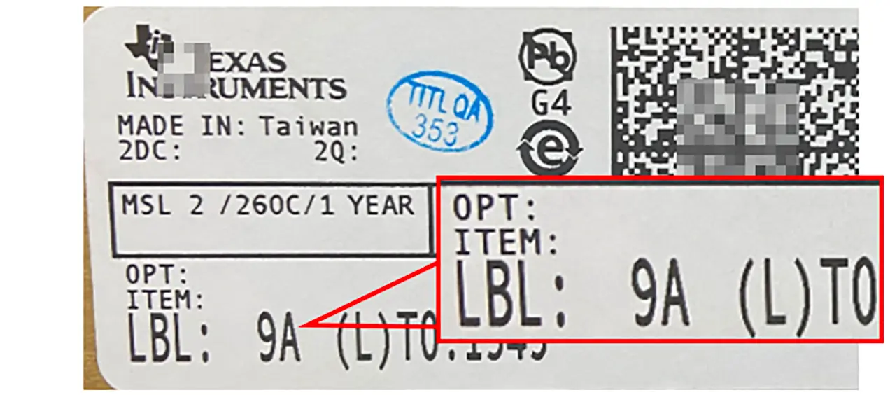
The lower left corner OPT and ITEM line spacing
(greater than) ITEM and LBL line spacing,
presenting a wide top and narrow bottom style.
The details of the end of the font can not be restored one-to-one, with the help of magnifying glasses and other tools can be identified.
Silkscreen Date Code Position in the Lower Left Corner
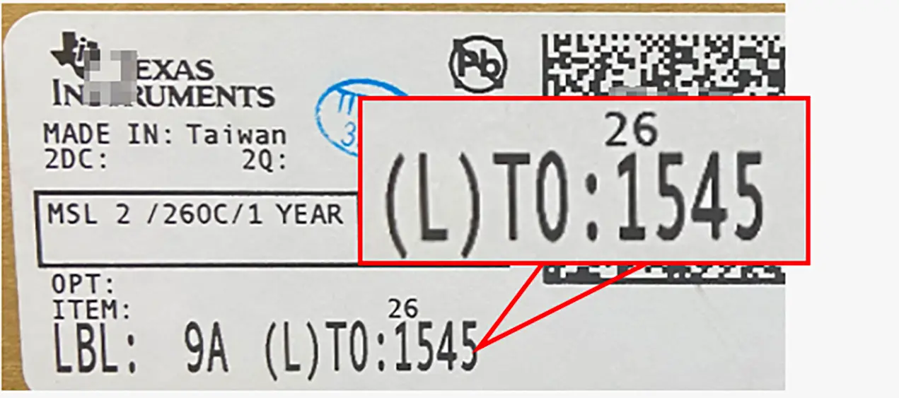
The first digit of the small silkscreen code is printed in front of the first digit below it.
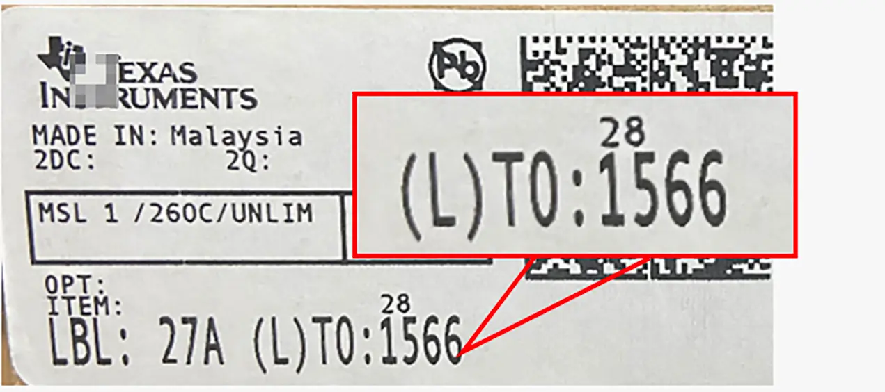
The printing position of the upper and lower digits appear aligned, etc.
Model Number and Quantity Printing Position
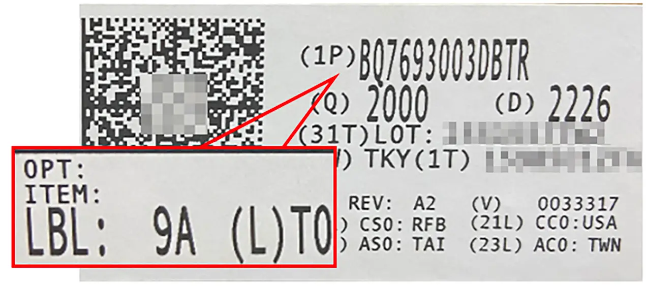
The first digit of (Q) will be aligned with or slightly in front of the second letter of (1P), and will not present alignment with the first letter of (1P).
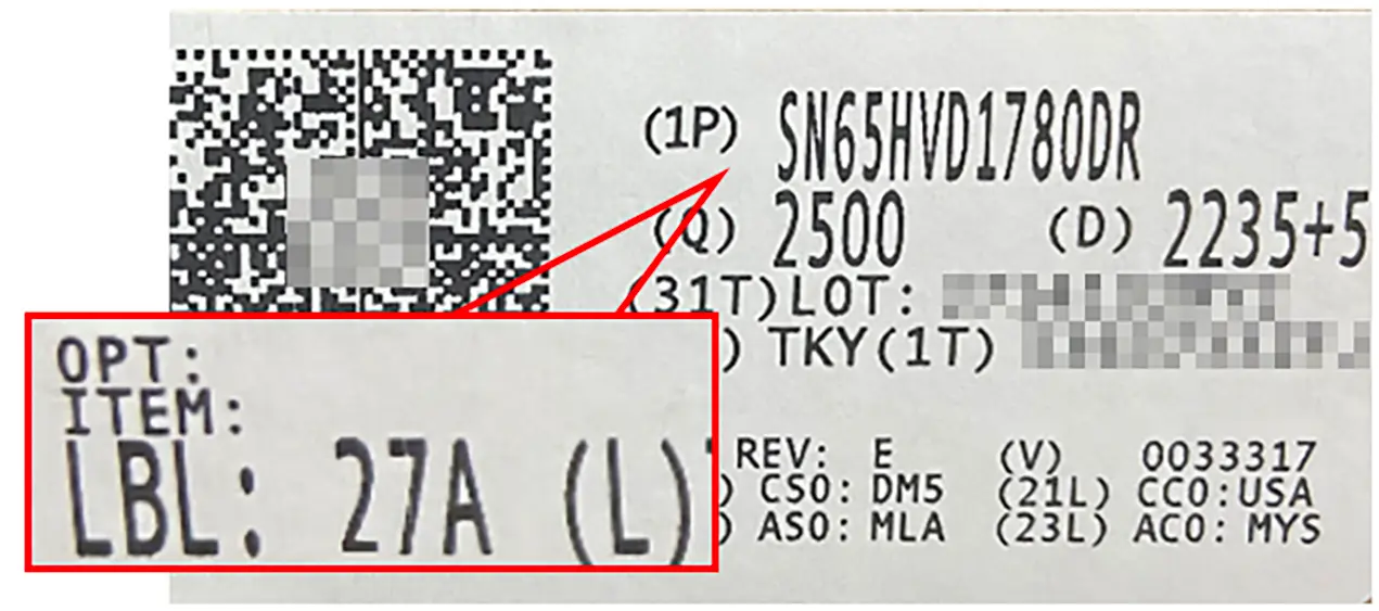
Q) and (1P) will appear aligned and so on.
Printed line spacing in the lower right corner
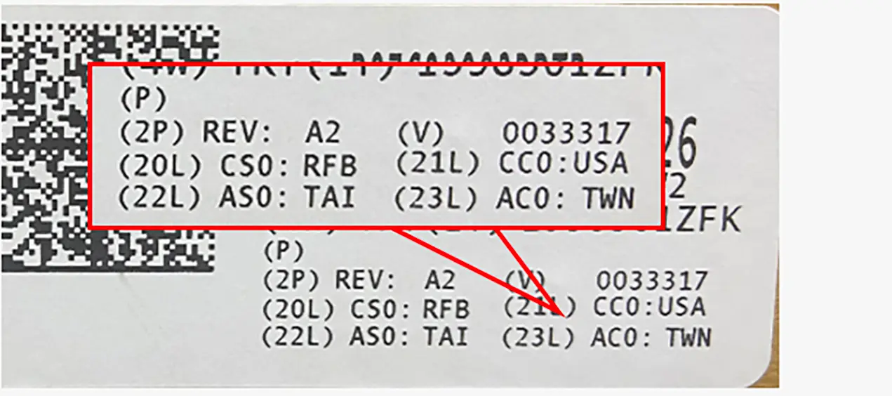
The spacing between the first and second lines in the lower right corner (greater than) the spacing between the second and third lines;
such as the spacing between REV and CSO (greater than)
the spacing between CSO and ASO.
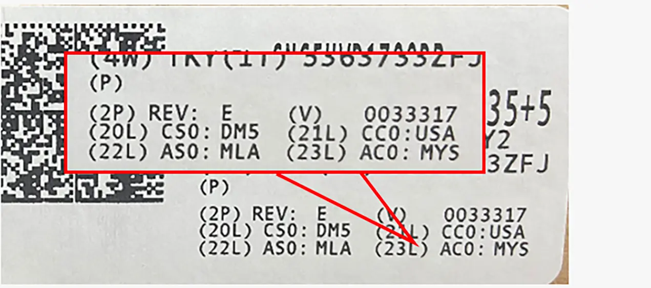
The printing line spacing presents parity or a large span between the upper and lower lines.
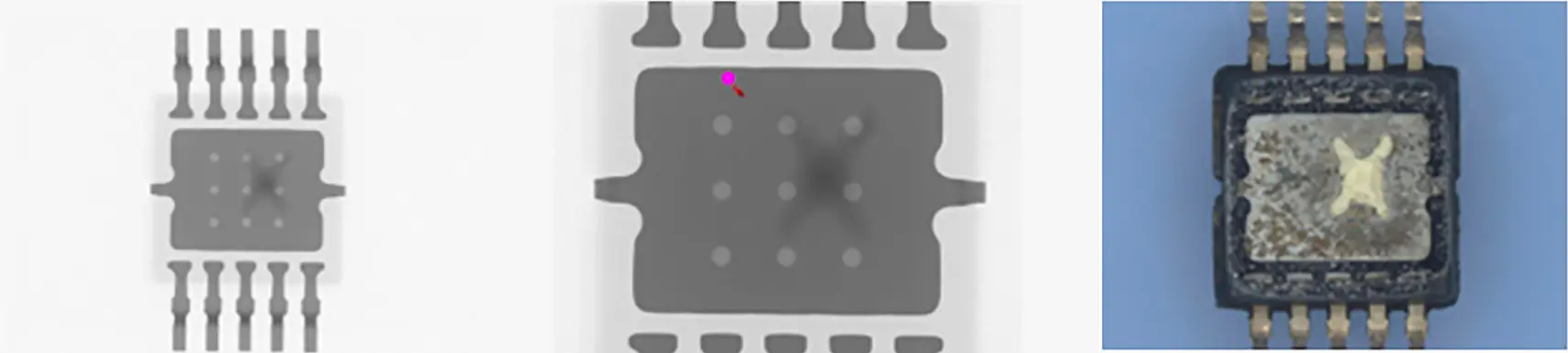
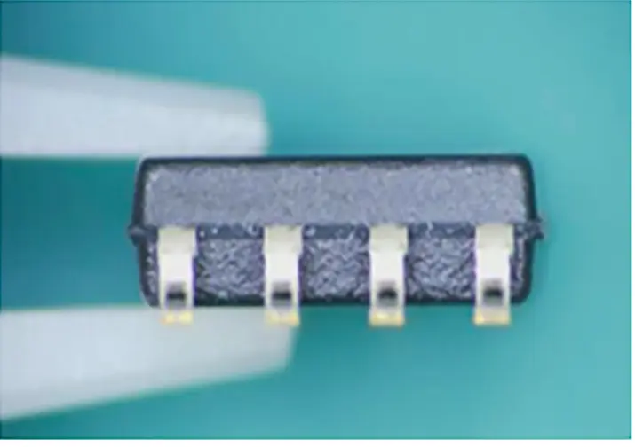
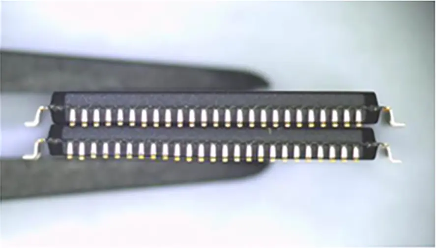
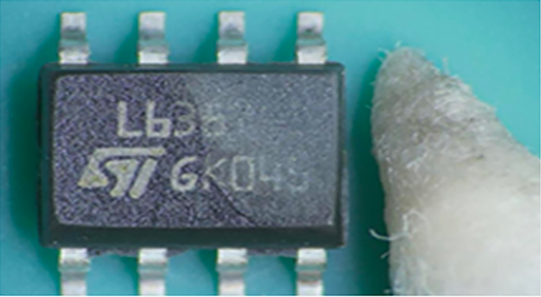
The Inspection of appearance mainly includes the chip’s silkscreen typing, verification of the date code, country of origin;
whether there is re-coating; the state of the PIN foot; whether there are re-polishing traces, unknown residues; the location
of the manufacturer LOGO.
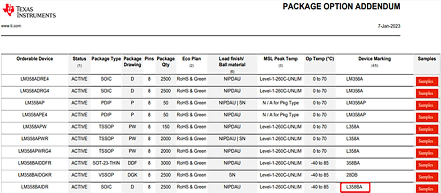
According to the official website corresponding to the
silk-screen marking instructions, verify the test material
silk-screen typing is consistent.
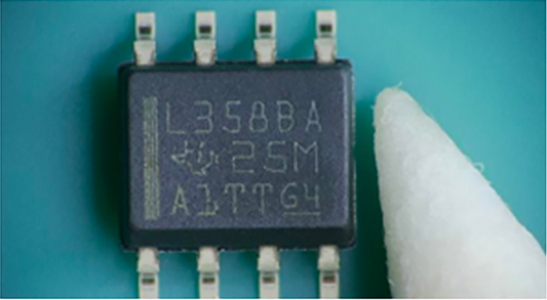
LM358BAIDR, the official website mark silkscreen typing for “L358BA”, and the physical consistency
Normal silkscreen printing; no re-coating traces; no traces of use of pin feet, etc.
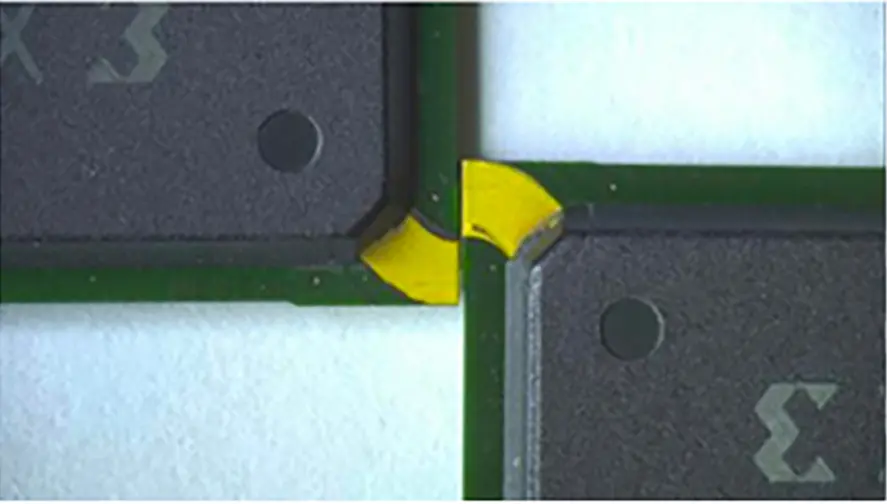
Pin feet with traces of use; residual scratches; change cover traces; silkscreen grinding marks;
silkscreen grinding marks; secondary coating traces of appearance, etc.
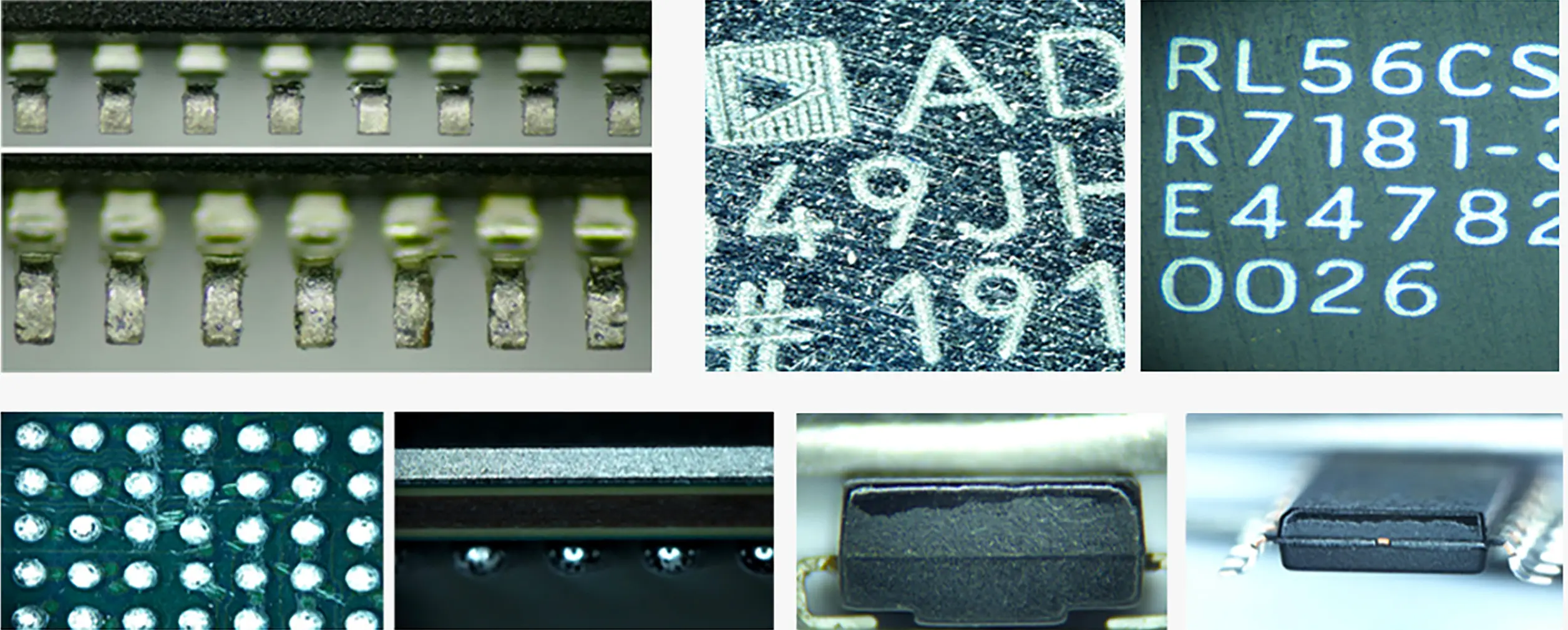
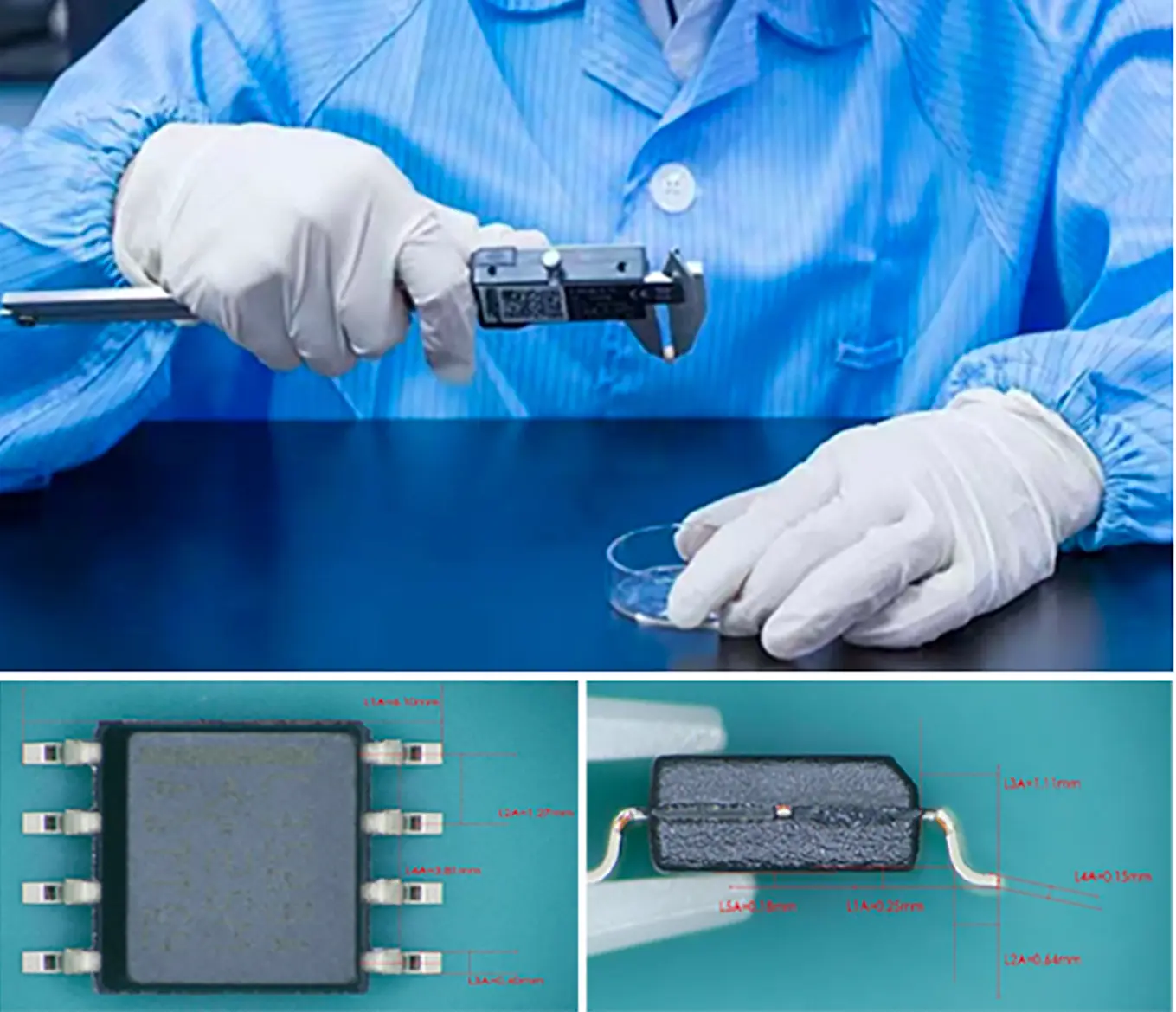
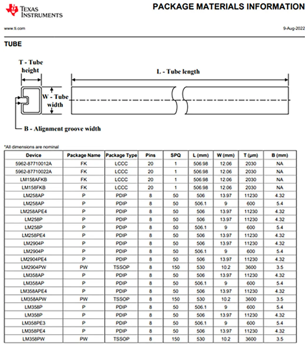
The chip size specifications are measured, according to the data in the specification on the official website
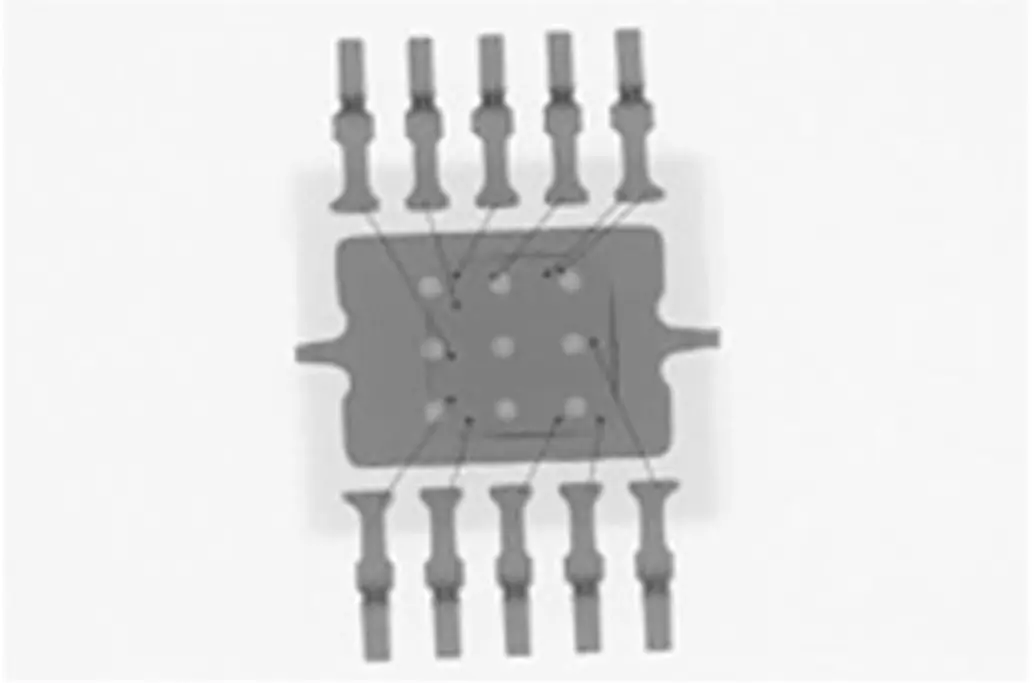
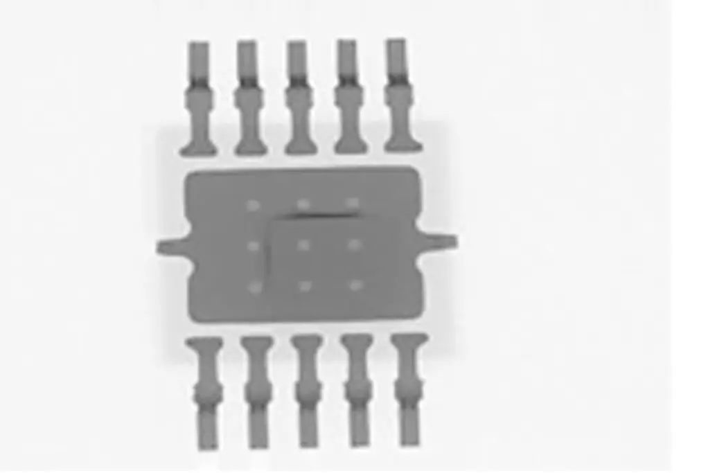
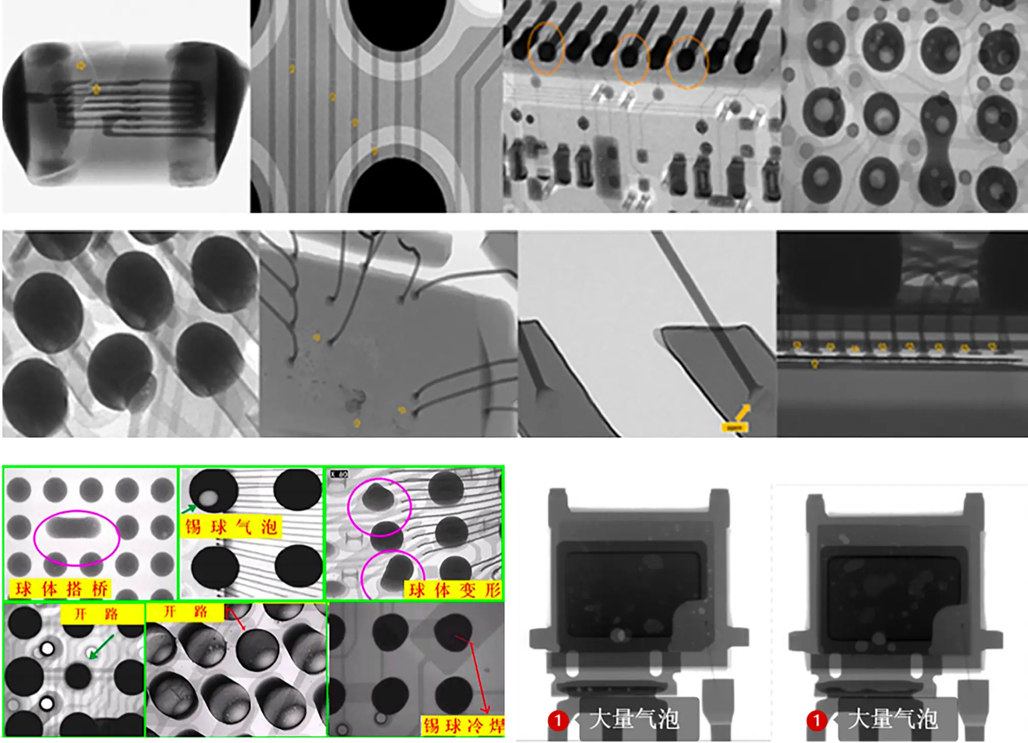
Detection of chip packaging defects, such as peeling layers, bursts, voids, punch line integrity, etc.
Detection of defects such as open circuits, short circuits or abnormal connections that may arise in connection lines.
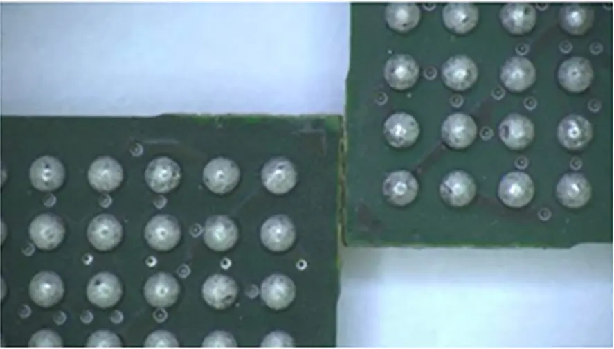
Detection of the integrity of the tin balls in the tin ball array package and in the overlay chip package.
Measurement of chip size, wire arc measurement, and measurement of the proportion of tin area eaten by components.

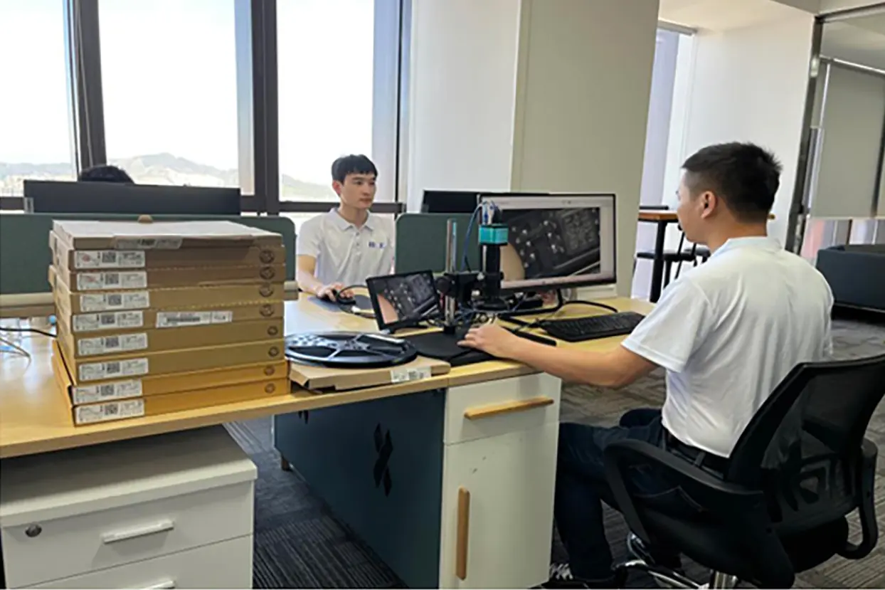
We will leave it to a third-party testing institution, which will issue an authoritative inspection report upon completion.

White Horse Laboratories

Shenzhen Juxin Testing Technology Co., Ltd
China Saibao Laboratory

Shenzhen Chuangxin Online Inspection Technology Co., Ltd
The lettering fades slightly after wiping, but there
is no obvious adverse phenomenon.
There are obvious signs of secondary coating on the surface, by wiping the surface of the chip with chemical reagents, black glue is found to have come off and the silkscreen receded.
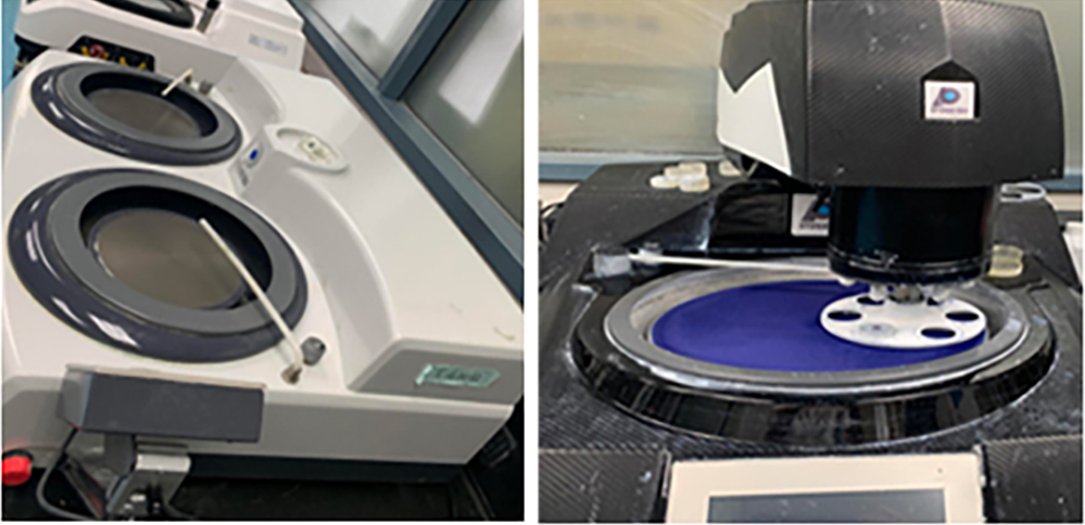
Description: After local grinding and polishing of the object to be tested, clear cross-sectional structure imaging can be
obtained, and whether there are defects inside it can be observed through high magnification microscope, and it is also
commonly used to check the PCBA welding situation, or as a pre-treatment for specific inspection items. The main process
includes: prefabricated sample; grinding; polishing; high magnification microscope observation, etc.
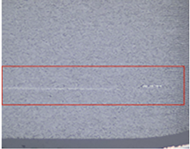
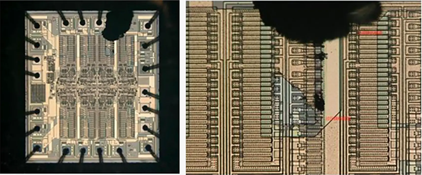
Electrode Layer Electrical Damage
Mechanical Damage
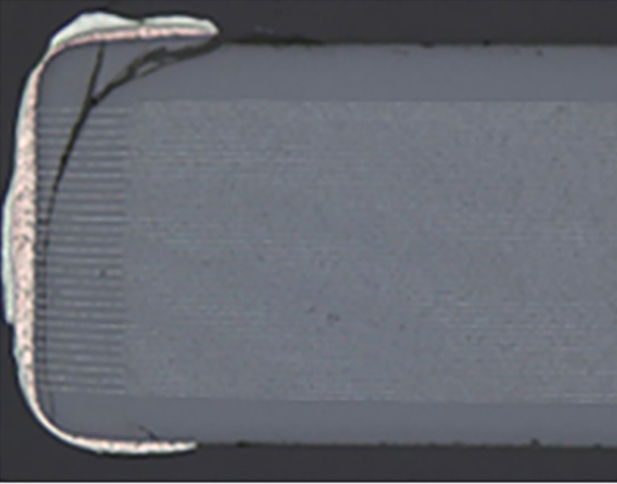
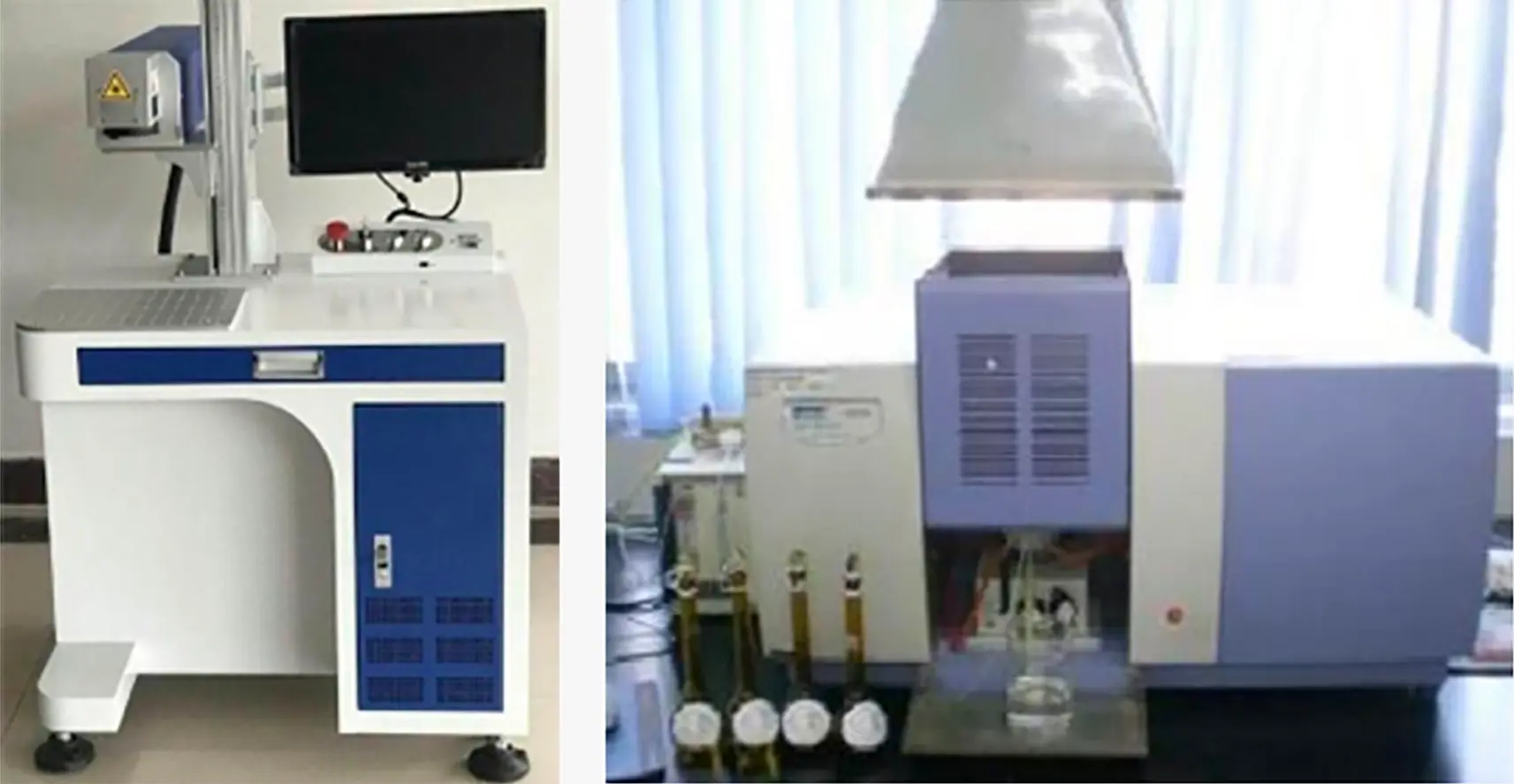
Laser etching and chemical etching are used to remove the outer layer of sealant, photoresist and other materials from the
component package, exposing the internal die and bonding lines. Through high magnification microscope or electron
microscope to observe the marking and printing information on the die surface, as well as the presence of process defects
or damage traces, commonly used in the original factory marking identification, but also for the failure device analysis of the
sample making process, to facilitate other testing projects.
The main processes include: X-ray positioning; laser debinding; chemical degum.
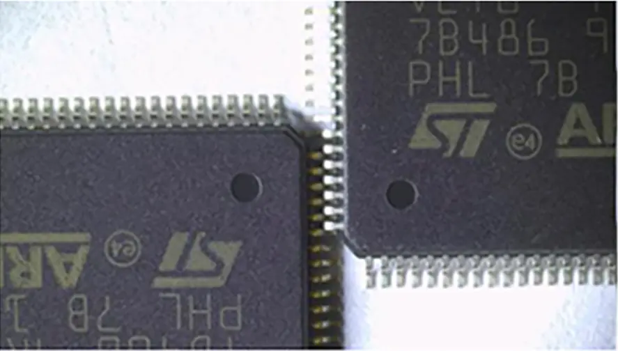
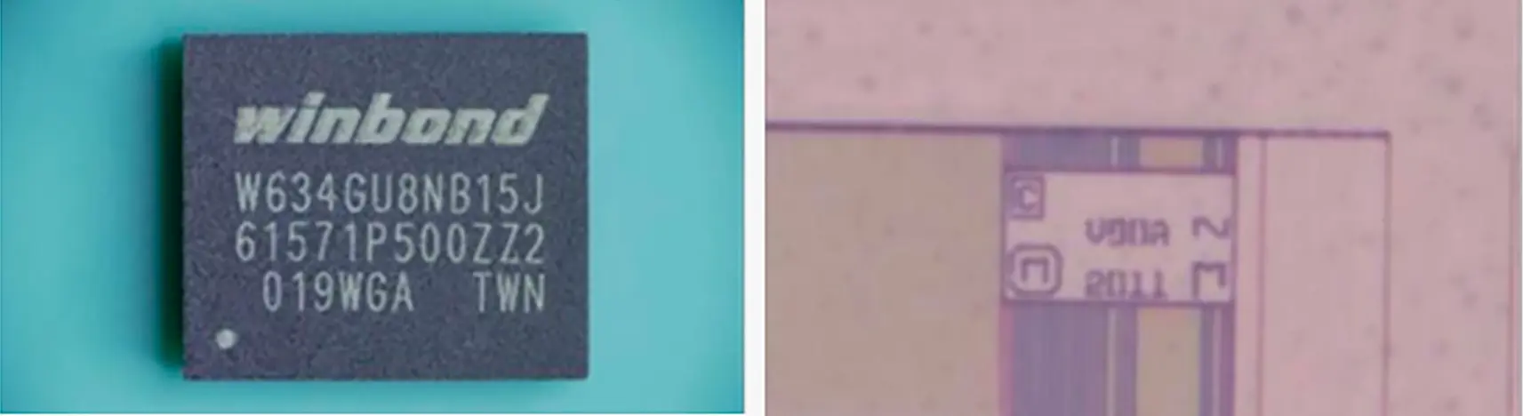
Counterfeit Replacement Wafers
Components of WINBOND, which come out of the open cover, are MICRON wafers.
The wafer surface has obvious electrical damage traces.
No wafers inside the sample.