TI TPS63802 high efficiency 2A high current buck b
TI公司的TPS63802高效大电流降压-升压转换器,其输入电压可高于,等于或低于输出电压.输出电流在很宽电压范围内高达2A.器件在升压模式峰值电流在4.5A,在降压模式为3.5A,输出电压可编程调整.能根据输入电压自动从降压变换到升压模式,当输入电压大约等于输出电压时器件维持3个周期的降压-升压模式.输入电压范围1.3V-5.5V,输出电压范围1.8V-5V(可调整).主要用在系统预稳压(智能手机,平板电脑,EFT终端和远程通信系统),点负载稳压(有线传感器,端口/线缆适配器和加密狗),指纹,面部ID,照相机传感器(智能手机,电子智能锁,IP网络照相机),RF放大器电源(智能传感器),热电设备(TCE/TEM)电源(数据通信,关模块,制冷/加热).本文介绍了TPS63802主要特性,功能框图和应用电路,以及评估模块TPS63802EVM主要特性,电路图,材料清单和PCB设计图.
The TPS63802 is a high efficiency, high outputcurrent buck-boost converter. It is used when theinput voltage is higher, equal, or lower than the outputvoltage. Output currents up to 2 A are supported overa wide voltage range. The device limits the peakcurrent at 4.5 A in Boost-Mode and 3.5 A in Buck-Mode. The device is adjusted to the programmed output voltage. It automatically changes from buck toboost operation based on the input voltage. Itremains in a 3-cycle buck-boost mode when the inputvoltage is approximately equal to the output voltage.
The transitions happen seamlessly and avoidsunwanted toggling within the modes. The TPS63802comes in a 2 mm x 3 mm package. The device workswith tiny passive components to keep the overallsolution size small.
TPS63802主要特性:
1• Input Voltage Range: 1.3 V to 5.5 V
– >1.8 V for Device Start-up
• Output Voltage Range: 1.8 V to 5 V (adjustable)
• 2-A Output Current for VIN ≥ 2.3 V, VOUT = 3.3 V
• High Efficiency Over the Entire Load Range
– Power Save Mode with Mode Selection
• Peak Current Buck-Boost Mode Architecture
– Seamless Transition Between Buck, Buck-Boost and Boost operation modes
– Operates With Low and High OutputCapacitance values
– Forward and Reverse Current Operation
– Start-up Into Pre-Biased Outputs
• Safety- and Robust Operation Features
– Integrated Soft Start
– Over-Temperature- and Over-Voltage-Protection
– True Shutdown Function with Load Disconnect
– Forward and Backward current limit
• Small Solution Size
– 2 mm x 3 mm Package size
– Small 0.47 μH inductor
– Works With 22μF Minimum Output Capacitor
• Create a Custom Design Using the TPS63802With the WEBENCH® Power Designer
TPS63802应用:
• System Pre-Regulator (Smartphone, Tablet, EFTTerminal, Telematics)
• Point-of-Load Regulation (Wired Sensor,Port/Cable Adapter and Dongle)
• Fingerprint, Face-ID, Camera Sensors(Smartphone, Electronic Smart Lock, IP Network Camera)
• RF Amplifier Supply (Smart Sensors)
• Thermoelectric Device (TEC/TEM) Supply(Datacom, Optical Modules, Cooling/Heating)
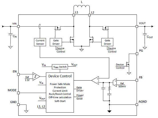
图1.TPS63802功能框图
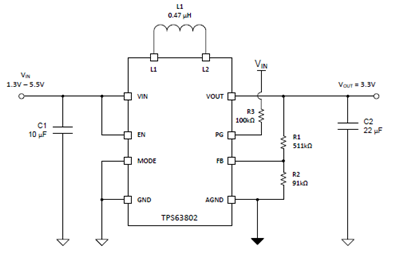
图2.TPS63802 3.3Vout应用电路图
评估模块TPS63802EVM
This user’s guide describes the operation, and use of the TPS63802EVM evaluation module (EVM). TheTPS63802EVM is designed to help the users easily evaluate and test the operation and functionality of theTPS63802 buck-boost converter. The TPS63802EVM has the output voltage set to 3.3 V. The EVMoperates from 1.3 V to 5.5 V input voltage. Output current can go up to 2 A in buck mode and boost mode.
This document includes setup instructions for the hardware, a schematic diagram, a bill of materials(BOM), and printed-circuit board (PCB) layout drawings for the evaluation module. Throughout thisdocument, the abbreviations EVM, TPS63802EVM, and the term evaluation module are synonymous withthe TPS63802, unless otherwise noted.
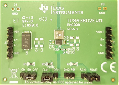
图3.评估模块TPS63802EVM外形图
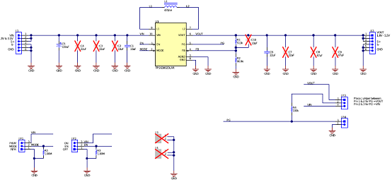
图4.评估模块TPS63802EVM电路图
评估模块TPS63802EVM材料清单:

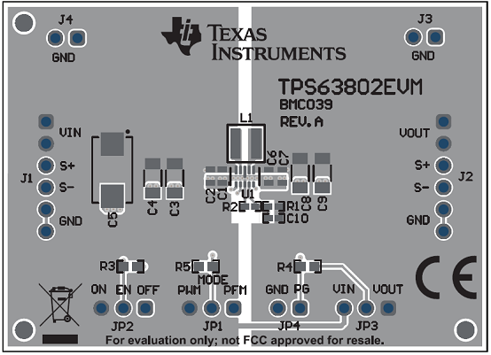
图5.评估模块TPS63802EVM PCB装配图
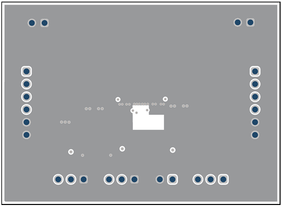
图6.评估模块TPS63802EVM PCB信号层1
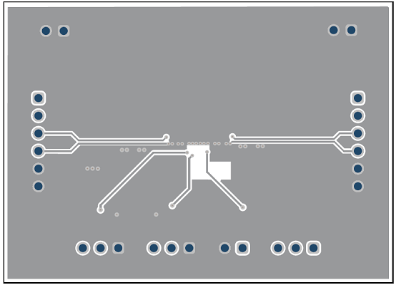
图7.评估模块TPS63802EVM PCB信号层2
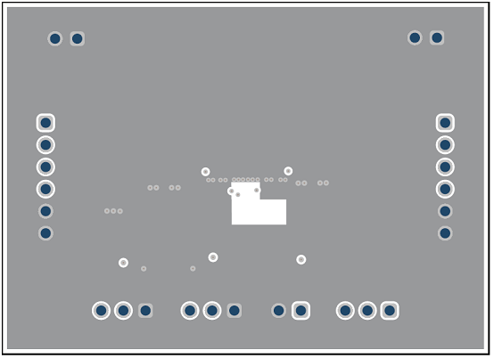
图8.评估模块TPS63802EVM PCB底层走线图
详情请见:
http://www.ti.com/lit/ds/symlink/tps63802.pdf
和http://www.ti.com/lit/ug/slvubh9b/slvubh9b.pdf
 tps63802.zip
 slvubh9b.pdf

